How does scanning electron microscopy work?

Ever wonder how we can see things so small, the human eye doesn't even know it exists? Today I'll be writing about how scanning electron microscopes allow us to see far beyond what traditional microscopes can provide. You see, optical microscopy (which uses visible light waves for imaging) only allows us to resolve features 250 nanometers and larger due to diffraction limitations. You can read more about this diffraction barrier here. Scanning electron microscopy is able to achieve a much finer resolution because we're basically shooting a focused beam of electrons at a sample instead of light, and this beam of electrons has a much smaller wavelength than visisble light, allowing us to greatly reduce the diffraction limitation.
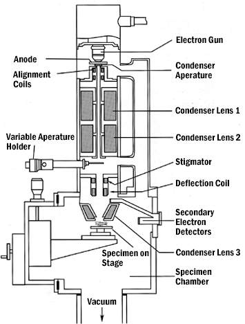
How the machine works
The picture below displays a schematic of a typical scanning electron microscope. Essentially, an electron beam is generated, focused, and then used to scan across a sample in a raster pattern.

The two main types of electron sources are thermionic and field emission. Thermionic sources typically use a tungsten filament which is heated to 2700 Kelvin, sufficient to overcome the filament’s work function, allowing electrons to exit the material and thus providing a source for an electron beam. Field emission sources take advantage of quantum tunneling to create an electron beam. Field emission sources are capable of producing sub-nanometer resolution images, however, this source type is much more expensive and usually cost prohibitive.
In order to achieve a sufficient electron mean free path, the SEM chamber must be pumped to low vacuum conditions. Generally, the length of the chamber is one meter, which requires pressures on the order of $10^{-4}$ torr. The electron beam passes through a number of electromagnetic lenses to demagnify and focus the beam, allowing a higher resolution for more detailed imaging. An objective aperture controls the electron beam by means of limiting electrons far from the beam center. A smaller aperture will shrink the electron probe radius, but will also reduce the current as it essentially removes the electrons not near the beam center. A stigmator is used to ensure the electron beam is not elliptical in nature, but perfectly round; this allows us for consistent imaging in all axises. Lastly, an objective lens is used to focus the electron beam onto the sample.
What you can learn from an SEM image
When the electron beam reaches the sample, a number of interactions occur. Some electrons elastically collide with and bounce back off the surface, known as backscattered electrons. This electron signal provides mainly compositional contrast. A grayscale image is created according to the number of backscattered electrons at each position; larger atoms will backscatter more electrons and thus be displayed brighter in the image.
Secondary electrons are produced by inelastic electron collisions with the lattice. For this interaction, an incident electron ejects an electron from the sample. The electron ejected from its resident shell in the sample is considered a secondary electron, and has considerably less energy than the incident electron. A similar grayscale image may be produced by counting the number of secondary electrons ejected at each position. Secondary electrons are the most commonly used signal from imaging and provide good topographical detail.
Elemental makeup of a sample can be determined by energy dispersive x-ray spectroscopy. When the high energy electron beam strikes the surface, it has the ability to eject an electron resident in the material from its shell. When an electron from a higher level energy shell drops to fill the created hole, it emits energy in the form of a light wave, usually in the x-ray range, which has an energy characteristic of the material’s discrete energy difference between levels. Thus, the emitted x-rays can be used to identify the different atoms which make up a material. X-ray signals at each position in the scanning area may be compiled to generate a compositional map of the area, which can be useful when identifying phases within a material.